
Product Center
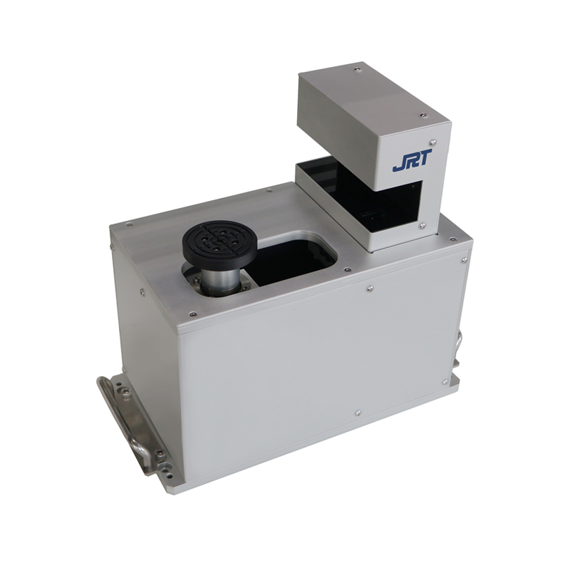
Compared to the standard version, the laser detection accuracy is higher
A new type of aligner suitable for wafers of different materials and sizes
Suitable for position calibration of different materials such as transparent and semi transparent wafers
Using a multifunctional ultra high precision CCD laser micrometer, an integrated design is adopted that integrates the controller and motor driver into the device body
Control mode: Ethernet port or parallel port I/O
Gap and edge shapes that do not meet SEMI specifications can also be customized for design
Can increase the Z-axis to meet the demand for wafer lifting and lowering
Standard Specifications | |
| The object being transported | Various materials, sizes transparent, semi transparent, opaque wafers 2 inches, 4 inches, 6 inches, 8 inches, 12 inches |
| Position accuracy | Wafer Center:±0.02 mm Wafer Notch, OF angle:±0.05 degrees |
| Time required for location determination | 5 seconds (excluding wafer retrieval time) |
| Sensor | Ultra high precision CCD laser micrometer |
| Position correction range | Within a radius of 10mm |
| Wafer adsorption method | Vacuum adsorption type |
| Cleanliness | ISO standard Class 2 (under independent exhaust conditions inside the drive structure) |
| Quality | Approximately 10 kg |
| Plant operations | Power supply:AC220V±10%5A Vacuum: Above -53 kPa |
Prev:Pre-Aligner
Next:No More!